In the world of light, shorter wavelengths unlock a new realm of possibilities. Deep ultraviolet (DUV) lasers, known for their razor-sharp precision and ultra-high energy photons, are the secret workhorses behind some of today’s most advanced technologies. From etching impossibly tiny circuits onto silicon wafers to probing the quantum mysteries of atoms and molecules, DUV lasers are critical tools powering innovation. Now, a team of researchers from the Chinese Academy of Sciences has taken a giant leap forward in this field, unveiling a revolutionary compact solid-state DUV laser system capable of producing highly coherent 193-nanometer (nm) light. This milestone, recently detailed in Advanced Photonics Nexus, could reshape the future of semiconductor manufacturing and more.
Why Deep Ultraviolet Lasers Matter
DUV lasers operate in a spectral region characterized by very short wavelengths—between 100 and 300 nm. At these wavelengths, light has high photon energy, which makes it ideal for applications requiring precision at microscopic and even atomic scales.
One of the most important industries relying on DUV lasers is semiconductor manufacturing. Modern microchips are created by a process called photolithography, where patterns are etched onto silicon wafers. The smaller the wavelength of light used in photolithography, the finer and more intricate these patterns can be, allowing for more powerful and efficient electronic devices. The 193-nm wavelength has become the industry standard for cutting-edge chip fabrication because it offers the resolution needed to produce the ultra-tiny features found in today’s processors and memory chips.
Traditional DUV sources, like gas-discharge lamps and bulky excimer lasers, have dominated the scene for years. But they come with serious downsides: they’re large, complex, consume vast amounts of power, and require high maintenance. What researchers have been chasing is a more compact, energy-efficient, and stable DUV source—and that’s precisely what the Chinese team has delivered.
The Breakthrough: Compact 193-nm Solid-State Laser System
The innovation lies in the researchers’ ability to produce 193-nm coherent light using a compact, solid-state laser platform. This system is not only more energy-efficient but also opens the door to simpler, more reliable designs that are easier to integrate into advanced manufacturing processes.
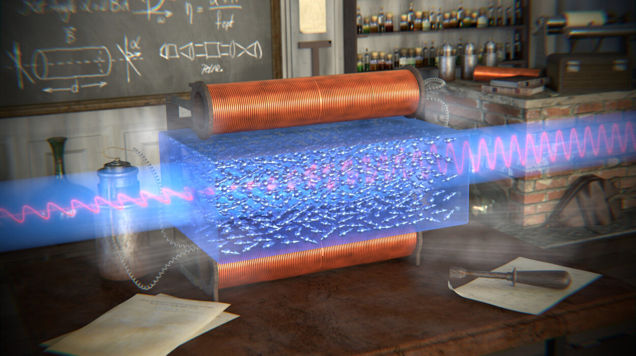
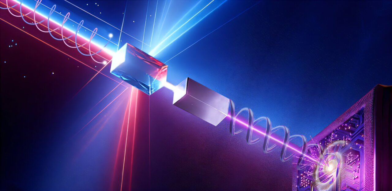
At the heart of their system is a homemade Yb:YAG (ytterbium-doped yttrium aluminum garnet) crystal amplifier. Yb:YAG is a powerful material commonly used in high-efficiency laser systems because of its excellent thermal properties and ability to deliver high average power. The amplifier generates a primary laser beam at 1,030 nm.
From there, the beam is split into two distinct paths:
- Path One: A portion of the beam undergoes fourth-harmonic generation (FHG), a nonlinear optical process that efficiently converts the 1,030-nm light into 258-nm ultraviolet light. The team achieved an impressive output power of 1.2 watts at this wavelength—no small feat given the energy losses typically encountered in such conversions.
- Path Two: The other portion of the 1,030-nm beam pumps an optical parametric amplifier (OPA), which produces a secondary beam at 1,553 nm with an output of 700 milliwatts. OPAs are prized for their ability to generate coherent light at different wavelengths through nonlinear optical processes, making them a powerful tool in wavelength conversion schemes.
These two beams—the 258-nm and the 1,553-nm—are then carefully combined inside cascaded lithium triborate (LBO) crystals. LBO is an ideal nonlinear crystal for frequency mixing because of its wide transparency range, high damage threshold, and excellent phase-matching properties. Through sum-frequency generation, these beams produce the final 193-nm deep ultraviolet light, with an average output power of 70 milliwatts and a narrow linewidth of less than 880 MHz. This level of precision and stability is a significant improvement over conventional excimer lasers.
A Vortex of Potential: The First 193-nm Vortex Beam
What truly sets this work apart, however, is the introduction of a vortex beam into the mix. The researchers incorporated a spiral phase plate into the 1,553-nm beam before combining it with the 258-nm beam. This clever addition transformed the beam into a vortex beam, meaning it carries orbital angular momentum (OAM).
Why does this matter? Vortex beams are twisted light waves that can impart angular momentum to microscopic particles. This makes them useful in applications ranging from optical tweezers, which manipulate tiny particles like cells or atoms, to advanced communications, where OAM can be used to encode more data onto a single beam of light.
Incredibly, this marks the first time a vortex beam has been demonstrated at the 193-nm wavelength using a solid-state laser system. The implications are huge. Vortex beams at this wavelength could pave the way for next-generation hybrid ArF excimer lasers (argon fluoride lasers commonly used in semiconductor lithography), adding new functionality and improving performance. They could also enable breakthroughs in defect inspection on semiconductor wafers, where precise control of light’s angular momentum allows for more sensitive and accurate detection of microscopic imperfections.
Additionally, 193-nm vortex beams could play a role in quantum communication systems, where encoding information in OAM states could dramatically increase data throughput and security. In optical micromanipulation, they offer unprecedented control in the movement and rotation of tiny particles, opening up new avenues in research and manufacturing.
A Compact Powerhouse for Advanced Manufacturing
Beyond its remarkable technical specifications, the compact nature of this laser system is a major advantage. Traditional excimer lasers are large, complex, and costly to maintain, requiring high-purity gases and regular component replacements. The solid-state system developed by the Chinese Academy of Sciences eliminates many of these issues, offering lower power consumption, increased reliability, and reduced maintenance needs.
For the semiconductor industry, this advancement could mean smaller, more cost-effective lithography tools, which in turn lowers manufacturing costs for advanced chips. As chipmakers face the enormous challenges of producing ever-smaller transistors (approaching the limits of Moore’s Law), innovations like this are crucial to keeping pace with the demand for faster, more efficient electronics.
Looking Ahead: The Future of DUV Laser Applications
While semiconductor lithography remains the most obvious application, the potential of this 193-nm laser system—and its vortex beam capabilities—extends far beyond chipmaking.
In high-resolution spectroscopy, DUV lasers are used to probe the electronic transitions of atoms and molecules with incredible precision. This is essential for fundamental research in physics and chemistry, including the study of quantum systems and the development of next-generation quantum technologies.
In precision material processing, DUV lasers can be employed to etch or drill materials with nanometer-scale accuracy, ideal for fabricating microelectromechanical systems (MEMS), biomedical devices, and nanoscale components.
In quantum communication and optical micromanipulation, the ability to produce vortex beams at deep ultraviolet wavelengths opens new doors. It allows for the exploration of quantum phenomena and the development of highly secure communication channels based on quantum encryption.
Conclusion: Shining a New Light on Tomorrow
The development of a compact 193-nm solid-state laser system by the Chinese Academy of Sciences represents a major milestone in laser physics and technology. It combines the precision and efficiency of modern solid-state systems with the powerful capabilities of deep ultraviolet light, offering a versatile tool for semiconductor lithography and much more.
The introduction of the 193-nm vortex beam is not just an impressive technical feat—it could be a game-changer, pushing the boundaries of what is possible in optical manipulation, quantum communication, and advanced manufacturing.
As industries race to produce smaller, faster, and more energy-efficient technologies, innovations like this laser system will play an essential role. With its reduced power consumption, compact design, and cutting-edge capabilities, it signals a bright future for both science and technology.
Reference: Zhitao Zhang et al, Compact narrow-linewidth solid-state 193-nm pulsed laser source utilizing an optical parametric amplifier and its vortex beam generation, Advanced Photonics Nexus (2025). DOI: 10.1117/1.APN.4.2.026011