Artificial Intelligence (AI) is at the heart of modern technological breakthroughs, from self-driving cars and intelligent virtual assistants to life-saving medical diagnostics. Yet, as AI systems become more complex and data-hungry, they increasingly run up against the same frustrating limits: energy inefficiencies and data bottlenecks. At the core of the problem lies one stubborn challenge—how to move enormous amounts of data between processing units quickly and efficiently without burning through energy like a gas-guzzling car.
Now, researchers at Columbia Engineering have unveiled a game-changing solution that could redefine the future of AI hardware. By blending the speed of light with advanced electronics, they’ve developed a revolutionary 3D photonic-electronic platform that crushes existing energy and bandwidth records. This innovation doesn’t just promise incremental gains—it signals a fundamental shift in how AI systems process and move information.
The groundbreaking study, “3D Photonics for Ultra-Low Energy, High Bandwidth-Density Chip Data Links,” spearheaded by Keren Bergman, Charles Batchelor Professor of Electrical Engineering at Columbia, was published in Nature Photonics. This isn’t just another research paper—it’s a blueprint for next-generation computing systems that could power everything from smarter AI to lightning-fast communication networks.
The Heart of the Problem: Data Movement Bottlenecks
AI has made remarkable strides, but behind the scenes, engineers are grappling with a major hurdle: data transfer bottlenecks. As AI models grow in complexity, they need to shuttle colossal amounts of data between different parts of a computer chip, or even between different servers. Moving that data consumes massive amounts of energy. Today’s systems are increasingly limited by the energy cost of transferring information rather than by the speed of computation itself.
Conventional data communication—whether inside a single chip or between chips in massive data centers—relies on electronic signals traveling through metal wires. These systems hit hard limits in both speed and efficiency. The more data you try to cram through, the more energy you burn, and the hotter the system gets. This creates an insurmountable wall for scaling up AI workloads, especially as we inch toward more distributed and parallel computing architectures.
“Increasing bandwidth without exponentially increasing energy has been a decades-long challenge,” says Keren Bergman. “Our team set out to rethink data movement entirely—and we believe this 3D photonic-electronic platform is the key.”
The Breakthrough: Marrying Light and Silicon in 3D
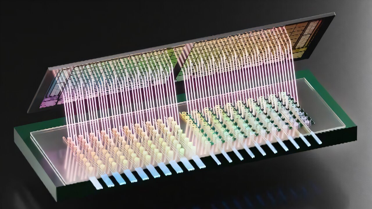
The Columbia Engineering team, working closely with Alyosha Christopher Molnar at Cornell University, has developed a 3D-integrated photonic-electronic chip. This platform merges the worlds of photonics—data transmitted by light—with tried-and-true complementary-metal-oxide-semiconductor (CMOS) electronics.
But why is this such a big deal?
Photonics allows data to travel at the speed of light using photons, rather than slow, energy-hungry electrons. Photonic data links offer massive bandwidth potential and vastly reduced energy consumption. Yet, integrating photonic components with traditional silicon electronics has historically been an expensive, complex challenge—until now.
The team’s innovation lies in vertically stacking 80 photonic transmitters and receivers within a tiny chip footprint using 3D integration techniques. They have created an ultra-compact and highly efficient data highway right inside the chip. This approach doesn’t just save space; it unlocks unprecedented energy and bandwidth efficiencies.
Here’s what makes this system a true marvel:
- Bandwidth: 800 gigabits per second (Gb/s)
- Energy Efficiency: Just 120 femtojoules per bit—orders of magnitude lower than conventional solutions
- Bandwidth Density: 5.3 terabits per second per square millimeter (Tb/s/mm²), dwarfing previous benchmarks
And all this has been achieved using commercially available manufacturing processes. That means this technology isn’t just an academic exercise—it’s scalable, cost-effective, and ready for real-world adoption.
Why It Matters: Powering the AI Systems of Tomorrow
The implications for AI—and computing as a whole—are profound.
AI systems are increasingly distributed, often spread across multiple chips or entire data centers. These distributed systems depend on moving massive amounts of data between processing units quickly and efficiently. Until now, the energy cost and latency of these data transfers limited AI scalability. Bergman’s team has effectively removed those limits.
By breaking free from traditional data locality constraints, AI architectures can now operate on an entirely new scale. Distributed AI systems—where computation is spread across vast networks of chips—become not only feasible but highly efficient. Large-scale AI models, such as those used in natural language processing, computer vision, and deep reinforcement learning, can benefit from ultra-fast, energy-sipping data transfers.
Imagine AI models that once needed enormous data centers to function now running on smaller, more energy-efficient systems, reducing operational costs and environmental impact. This technology could power the next wave of autonomous vehicles, real-time medical diagnostics, and edge computing devices, all demanding rapid data processing with minimal energy use.
Beyond AI: Transforming the Entire Computing Ecosystem
While AI is the headline, the ripple effects of this innovation extend far beyond.
- High-Performance Computing (HPC): Supercomputers tackling climate modeling, drug discovery, and complex simulations require vast data bandwidth and energy efficiency. This technology could revolutionize HPC systems by enabling faster and more energy-efficient communication between compute nodes.
- Telecommunications: As global data traffic explodes, telecom networks are straining to keep up. Photonic-electronic platforms could support the ultra-fast data links needed for next-generation 6G networks, reducing latency and energy consumption for data-intensive applications like streaming and virtual reality.
- Disaggregated Memory Systems: Modern computing increasingly separates storage, memory, and compute units into modular, flexible architectures. The ability to transfer data seamlessly between these components, without energy bottlenecks, is critical. Columbia’s 3D photonic-electronic platform makes memory disaggregation more practical and efficient.
Collaboration and Vision: A Blueprint for the Future
The success of this project is also a testament to collaborative innovation. The Columbia Engineering team worked closely with Cornell’s Molnar lab, the Air Force Research Laboratory, and Dartmouth College. Together, they combined expertise in photonics, electronics, and systems engineering to solve one of computing’s most stubborn problems.
“We’re not just offering an incremental improvement,” says Bergman. “This work opens the door to entirely new architectures for AI and computing. The possibilities are endless.”
Their vision for the future includes:
- Scalable, energy-efficient AI systems
- Compact, high-performance computing platforms
- Sustainable, green data centers that reduce carbon footprints
- Next-generation wireless and wired communication networks
And the best part? This is not decades away. Because the technology leverages standard CMOS manufacturing, its path to commercialization is clear. Companies building AI accelerators, network processors, and cloud infrastructure could integrate these photonic-electronic platforms into their products sooner than we might expect.
The Takeaway: A New Era in Computing Has Begun
The 3D photonic-electronic platform developed by Columbia Engineering represents a paradigm shift. It shatters energy efficiency records, boosts bandwidth to unprecedented levels, and removes long-standing barriers to scaling up AI systems.
In a world increasingly reliant on data-driven technologies, energy efficiency isn’t just a bonus—it’s a necessity. This innovation points to a future where AI systems aren’t hobbled by energy constraints but are free to reach their full potential. And with scalable, industry-ready solutions in hand, that future might arrive sooner than we think.
As Keren Bergman puts it, “We’ve cracked the code on energy-efficient data movement. Now, it’s time to build the AI systems of tomorrow.”
Reference: Stuart Daudlin et al, 3D Photonics for Ultra-Low Energy, High Bandwidth-Density Chip Data Links, Nature Photonics (2025). DOI: 10.1038/s41566-025-01633-0 . On arXiv: DOI: 10.48550/arxiv.2310.01615