In a significant advancement in the field of additive manufacturing, researchers have achieved an extraordinary milestone in high-speed laser writing by creating lines spaced just 100 nm apart on a glass substrate. This breakthrough, published in the journal Optics Letters, demonstrates the potential of optimized direct laser writing (DLW) techniques to enable the production of super-resolution 3D structures. These advancements hold immense promise for the future of microlenses, photonic crystals, micro-optical devices, metamaterials, and other cutting-edge technologies.
DLW, a sophisticated technique in the realm of nanofabrication, employs a focused laser beam to selectively polymerize or solidify materials with nanoscale precision. This technique, often using multi-photon polymerization, is known for its ability to create highly precise and intricate 3D structures by focusing intense laser light at specific points in a photosensitive material. However, achieving extremely high-resolution patterns has been a longstanding challenge due to the inherent limitations of laser exposure, especially when attempting to print at smaller scales.
Overcoming the Challenges of High-Resolution Printing
According to Qiulan Liu, a researcher from Zhejiang Lab and Zhejiang University in China, the key challenge in achieving higher resolution in DLW lies in the intense laser light itself. “Increasing the resolution—the minimum distance between two adjacent features—is difficult because the intense laser light can cause unwanted exposure in nearby areas during DLW,” Liu explains.
In their breakthrough work, Liu and colleagues employed a novel approach that involved a dual-beam optical setup and a specialized photoresist material to overcome this challenge. The result was super-resolution DLW with lateral resolution as fine as 100 nm. Notably, this level of resolution was achieved while maintaining relatively high printing speeds, an important factor for real-world applications.
The optimized DLW technique demonstrated that 100-nm resolution could be maintained even at a 100 µm/s printing speed, and at 1000 µm/s, the resolution still reached 120 nm. These results suggest that the technique not only achieves unprecedented resolution but does so at impressive speeds, offering a pathway to rapidly fabricate complex optical elements with high precision.
Applications in Next-Generation Technologies
One of the most exciting applications of this high-resolution DLW technique is in the development of optical waveguide devices for virtual reality (VR) and augmented reality (AR) displays. These immersive technologies require precise, high-resolution structuring to produce the complex optical elements that are critical for their performance. The new technique offers a way to fabricate these devices quickly and with a level of accuracy that was previously unattainable.
Liu emphasizes the potential of this technology to revolutionize how optical devices are designed and manufactured for cutting-edge technologies. “This fast and high-precision approach allows rapid fabrication of complex optical elements, which are crucial for the performance of next-generation immersive technologies,” he notes.
Dual-Beam Optical Setup and Peripheral Photoinhibition
The researchers’ breakthrough in super-resolution DLW stemmed from a combination of innovative techniques. One of the key elements was their use of dual-beam optical setup and peripheral photoinhibition, a method that uses an inhibition beam to suppress unwanted polymerization at the edges of the laser-exposed area. This prevents the laser from exposing areas outside the intended pattern, allowing for much finer control over the writing process.
In addition, the researchers developed a specialized photoresist system to enhance the resolution further. The system consisted of a widely used monomer called PETA combined with a radical quencher known as BTPOS (Bis(2,2,6,6-tetramethyl-4-piperidyl-1-oxyl) sebacate). The BTPOS radical quencher helped reduce crosslinking, a phenomenon that often occurs when DLW is used to create high-resolution patterns. Crosslinking can cause unwanted bonding between polymer chains, which can lead to inaccuracies in the printed structures. By minimizing this effect, the researchers were able to produce more accurate, finely detailed patterns.
The experimental setup used a 525-nm femtosecond laser for excitation and a 532-nm picosecond laser for inhibition. These lasers were carefully coordinated through a picosecond delay unit to introduce a 2700 ps delay, accounting for the difference in the optical paths of the two beams. This delay was essential in ensuring that the inhibition beam acted precisely when needed, preventing unwanted polymerization and allowing for high-precision patterning.
To further enhance the quality of the writing process, the team employed a spatial light modulator (SLM) to modulate both the excitation and inhibition light. Additionally, they applied Zernike polynomials to the SLM to correct any wavefront aberrations that might arise during the writing process. This allowed for even greater control over the laser focus and ensured that the system remained stable throughout the experiments.
Fabricating Tiny Structures with High Precision
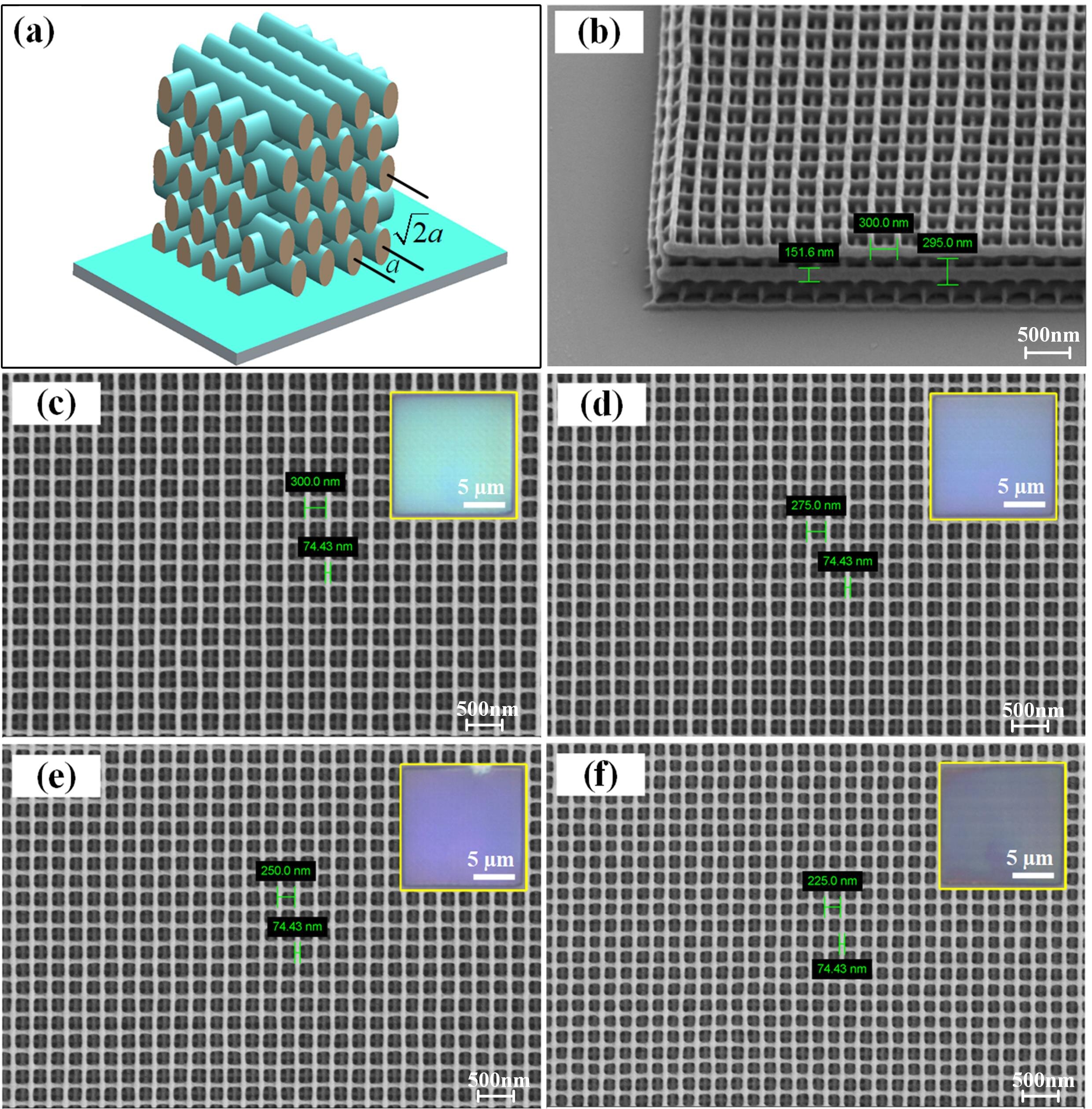
The team conducted several experiments to demonstrate the speed and resolution of their new DLW technique. Among their accomplishments, they successfully fabricated tiny 3D woodpile structures with lateral rod spacing ranging from 300 nm to 225 nm. The smallest axial period between the woodpile layers was 318 nm, which is remarkably close to the diffraction-limited axial resolution of 320 nm. This diffraction limit is determined by the wavelength of the laser light and the optical system’s ability to focus the laser beam. Achieving this level of resolution represents a significant step forward in the field of nanofabrication.

The success of these experiments underscores the capability of the new DLW technique to create intricate and highly detailed 3D structures at the nanoscale. Such precision is essential for the development of complex optical components, and the ability to produce these structures at high speeds could have a transformative impact on a wide range of industries.
Future Directions and Challenges
While the team’s results are impressive, they are not resting on their laurels. The researchers are already working on further improvements to the technology, with an eye toward increasing writing speeds even more. Their next goal is to reach speeds of 10 mm/s and 100 mm/s while maintaining the high resolution and quality of their printed structures. Achieving these speeds would make the technique even more practical for industrial applications, where rapid production is essential.
In addition to increasing the speed, the team is focused on improving the stability and practicality of their photoresist system. Stability is a critical factor in DLW, as even small variations in laser power, focus alignment, or optical system drift can lead to inaccuracies in the printed structures. By refining their photoresist system and optimizing the entire setup, the researchers aim to make super-resolution DLW a reliable and commercially viable technique for producing advanced optical devices.
Conclusion
The research team’s breakthrough in high-speed, high-resolution direct laser writing marks a significant milestone in the field of nanofabrication. By achieving an incredible 100-nm resolution and demonstrating the ability to print complex 3D structures with high precision and speed, they have opened the door to a wide range of applications, from microlenses to metamaterials to virtual and augmented reality devices.
This new approach holds the promise of accelerating the development of next-generation optical devices and manufacturing techniques. As the researchers continue to refine their methods and push the boundaries of what is possible with DLW, it is clear that this technology will play a central role in shaping the future of advanced optics, immersive technologies, and nanofabrication. The future of super-resolution 3D printing is bright, and the innovations coming out of this research will undoubtedly lead to breakthroughs in fields ranging from photonics to biomedical engineering to electronics.
Reference: Xi Liu et al, Super-resolution direct laser writing via multiphoton and peripheral photoinhibition photolithography, Optics Letters (2025). DOI: 10.1364/OL.552034